Test chip, GeoBox, PFM, Dec 7 2000
1 |
2 |
3 |
4 |
5 |
6 |
7 |
8 |
9 |
10 |
11 |
12 |
13 |
14 |

15 |

16 |
17 |
18 |
19 |
20 |
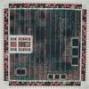
- Plot of the 0.18um test chip. 64x64 RAMs on right, 32x32 RAMs on bottom, CAM on bottom left, DLL on left
- CLK block with frequency multiplier on left and DLL on right
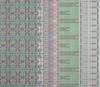
- Close up of RAM array
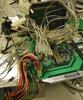
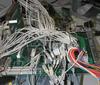
- Test chip debug board with logic analyser leads attached
- Another view of the board --- our low cost chip tester
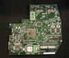
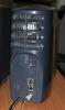
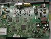
- GeoBox receiver PCB with ChipA, QED MIPS processor, Xilinx FPGA visible
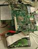
- GeoBox PCB with Geocast's system controller chip near the large white PCI slot on the left
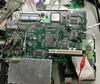
- Another picture of the board showing the 2 digital TV receivers in the metal can
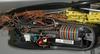
- GeoBox with bottom removed. PCB on top of chassis and hard drive/power supply mounted on other side. The fine wires attach to thermocouples to measure temperature inside enclosure
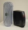
- GeoBox from trial manufacturing run
- Rear of the GeoBox. Power cable, antenna cable, USB and ethernet connectors, smart card slot. Fan inside grille
- Our high-gain digital TV antenna. Circuit board inside is powered through the coax cable
- GeoBrick and antenna setup
- The guts of an Echostar satellite receiver box. Smart card is on the bottom left
- Mira in dad's office
- Playing mover in dad's office
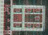
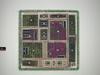
- Plot of PFM. Blocks are:
| front-end | glue-logic | serial controller | PCI |
| deinterleaver | smart card | data streaming | |
| Reed-Solomon | PID filter | data streaming | PCI |
| memory controller | | DLL+clk mult+DLL | JTAG |
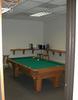
- Pool room
- Break room
- Well stocks cupboard for the engineers